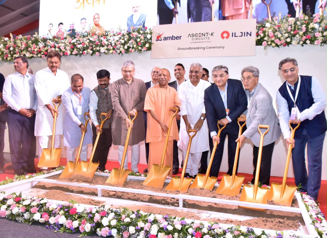
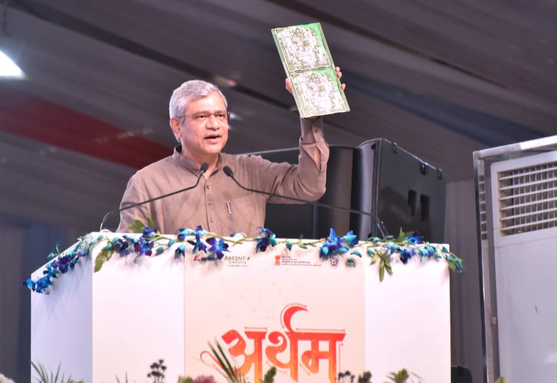
Gautam Buddha Nagar , June 27, 2026: Union Minister for Electronics & Information Technology, Railways and Information & Broadcasting Ashwini Vaishnaw said that India will soon begin domestic manufacturing of advanced Printed Circuit Boards (PCBs) worth nearly ₹40,000 crore, reducing dependence on imports and strengthening the country’s electronics ecosystem.
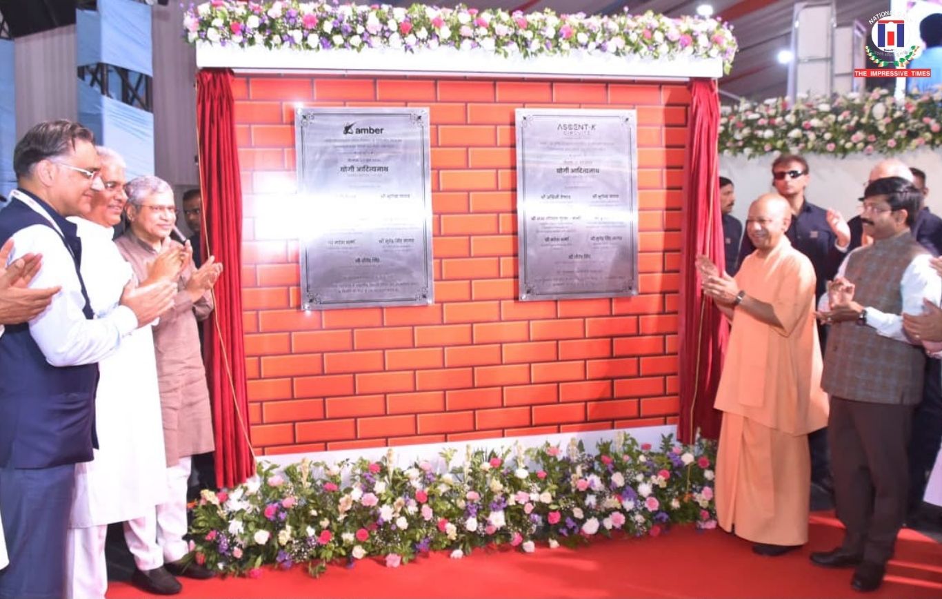
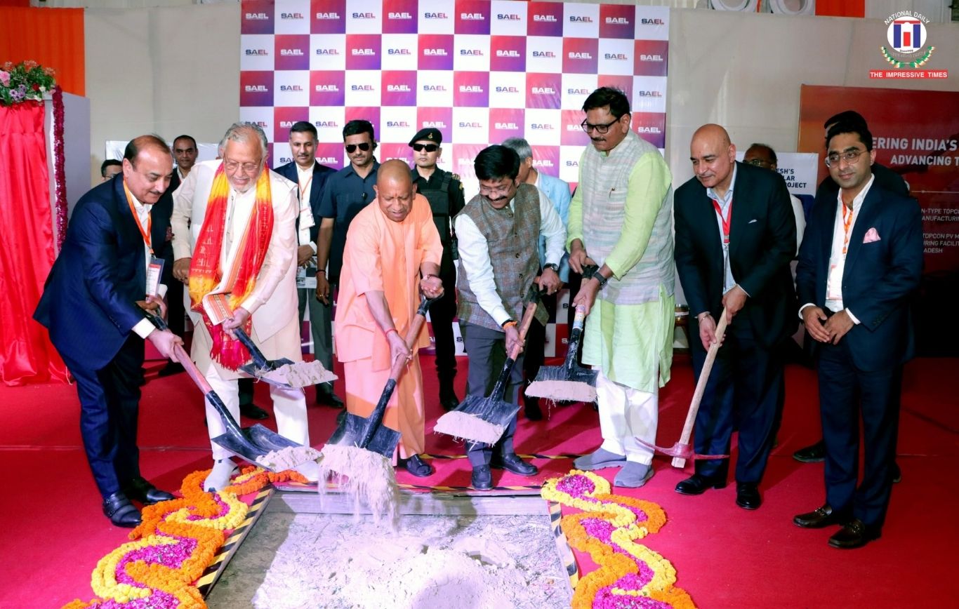
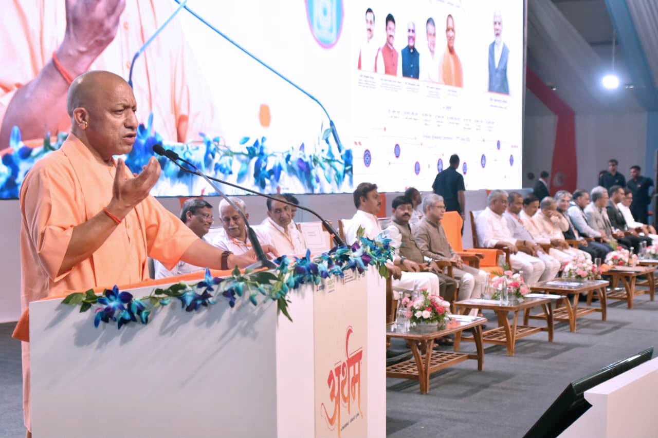
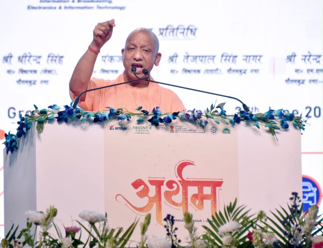
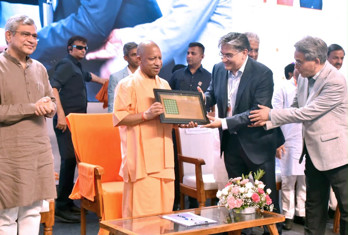
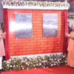
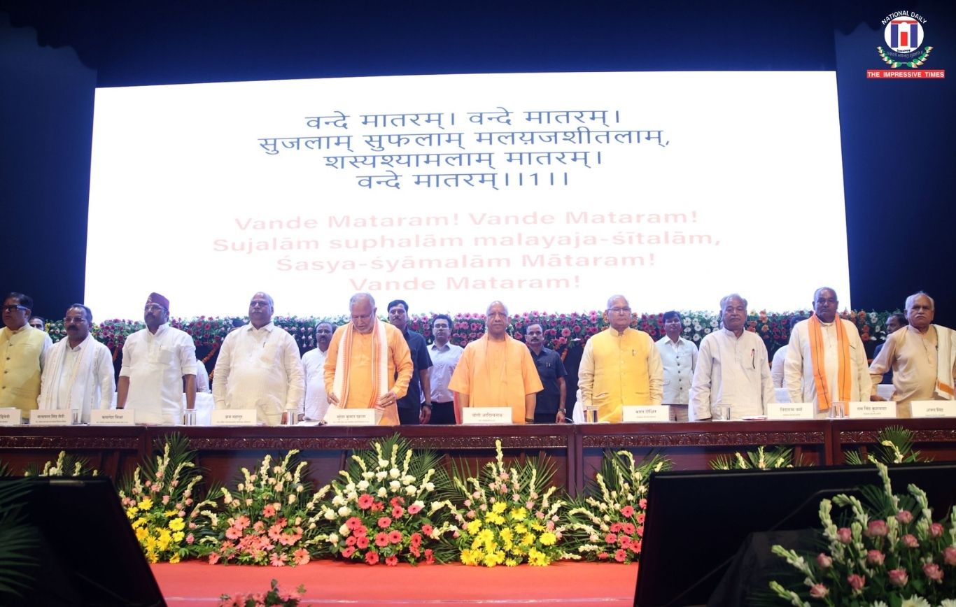
The announcement was made during the foundation stone ceremony of two major electronics manufacturing projects worth around ₹6,750 crore at Yamuna City, Jewar, in Gautam Buddha Nagar district. The projects were launched jointly by Uttar Pradesh Chief Minister Yogi Adityanath and Union Minister Ashwini Vaishnaw.
Addressing the gathering, Ashwini Vaishnaw said Jewar is set to emerge as a key destination for electronics and semiconductor manufacturing in India. He highlighted that the upcoming facilities will produce advanced multi-layer PCBs, which are essential components in modern electronic devices.
He explained that these high-end PCBs contain multiple layers of integrated circuits packed into compact structures and serve as the foundation for various electronic products. The minister said manufacturing such critical components within India will boost self-reliance, conserve foreign exchange and create opportunities for supporting industries.
The Union Minister further stated that Jewar’s growth as an electronics manufacturing centre, along with the expanding semiconductor ecosystem, will help Uttar Pradesh become one of the leading technology manufacturing destinations in the country.
Highlighting infrastructure development, Ashwini Vaishnaw said the proposed Delhi-Lucknow-Varanasi-Patna-Siliguri Bullet Train corridor will significantly improve connectivity and support industrial growth. He added that travel between Delhi and Lucknow through the bullet train will reduce to around 2 hours and 10 minutes, while Jewar to Lucknow will take approximately 1 hour and 40 minutes.
During the programme, Chief Minister Yogi Adityanath also laid the foundation stone for the first industrial unit in the Electronics Manufacturing Cluster (EMC) at Sector-10 of the Yamuna Expressway Industrial Development Authority area.
The 206-acre Electronics Manufacturing Cluster is being developed at an estimated cost of ₹417 crore with support from the Government of India, including a central contribution of ₹144 crore. The project is expected to attract further investments, create skilled employment and strengthen the electronics supply chain.
The beginning of advanced PCB manufacturing in India marks a major step towards reducing import dependency in critical electronic components. Officials said the move will encourage domestic value addition, support ancillary industries and help Indian manufacturers compete in global markets.
The expansion of India’s semiconductor and electronics ecosystem is being supported through the India Semiconductor Mission, which aims to build a complete manufacturing and design ecosystem. The initiative focuses on chip fabrication, packaging, semiconductor design, equipment development and resilient supply chains to establish India as a global electronics manufacturing hub.


No Comments: