India’s first advanced 3D semiconductor packaging unit launched in Odisha; major push for AI, 5G and defence electronics
Foundation laid at Info Valley Bhubaneswar as state emerges as key hub in semiconductor ecosystem
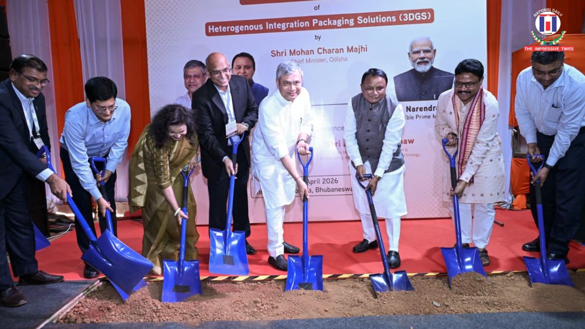
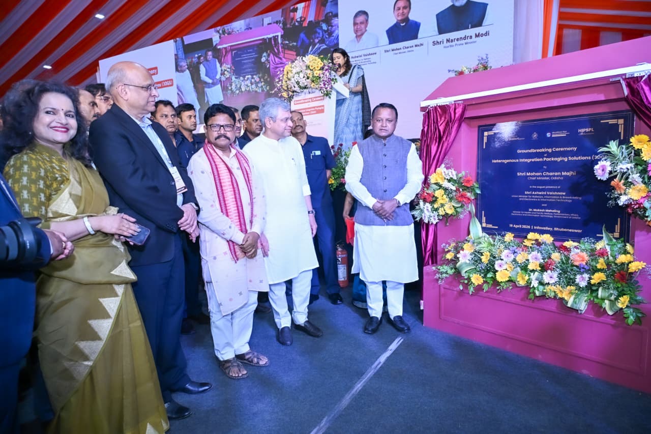
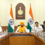
Bhubaneswar, April 19, 2026: The foundation stone for India’s first advanced 3D semiconductor packaging unit was laid at Info Valley in Bhubaneswar, marking a major milestone in the country’s semiconductor and electronics manufacturing journey and strengthening Odisha’s position as an emerging technology hub.
The project, promoted by 3D Glass Solutions through its Indian subsidiary Heterogeneous Integration Packaging Solutions Private Limited, is aimed at building a next generation heterogeneous integration packaging facility in India.
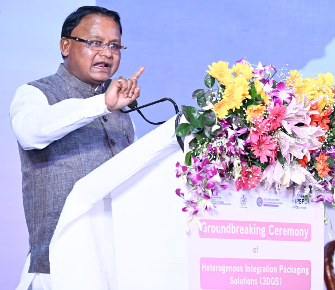
Chief Minister Mohan Charan Majhi described the project as a historic development for both Odisha and the country, stating that it aligns with the vision of Prime Minister Narendra Modi for Atmanirbhar Bharat in high technology manufacturing.
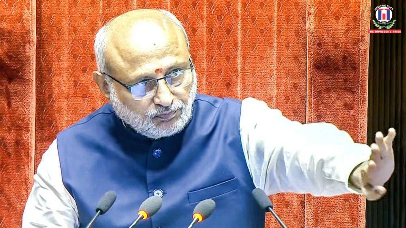
Union Minister Ashwini Vaishnaw said Odisha is rapidly transforming from a resource based economy into a strong player in electronics, IT and semiconductor manufacturing sectors.
He highlighted that India’s electronics manufacturing output has grown significantly over the past decade, with the country now becoming a major global hub for mobile phone production and exports.
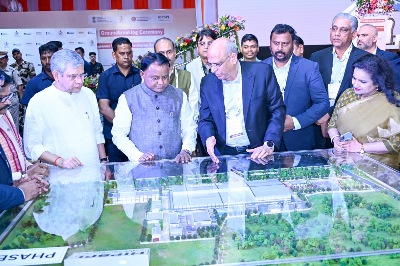
The new facility is expected to manufacture advanced 3D glass substrate based semiconductor packaging solutions, which are critical for next generation technologies including artificial intelligence, high performance computing and advanced defence systems.
Officials said the project represents one of the most sophisticated chip packaging technologies being developed in India and will strengthen the domestic semiconductor value chain.
The total investment in the project is approximately ₹1,943 crore, with support from both the central and state governments to encourage high technology manufacturing.The facility is expected to produce large volumes of advanced semiconductor packaging units annually, catering to global demand in emerging technology sectors.
The project is also expected to generate significant employment opportunities for engineers, diploma holders and skilled technicians in Odisha.Authorities said the initiative will help transform the state into a technology driven industrial hub by attracting global investment in semiconductor manufacturing.
The facility will serve key sectors such as artificial intelligence, machine learning, 5G and 6G communications, automotive electronics, aerospace and defence technologies.Union Minister Ashwini Vaishnaw said multiple semiconductor and electronics projects are already in development in Odisha under national missions, with more proposals under consideration.
He also noted that large scale railway infrastructure expansion and industrial investments are further strengthening Odisha’s economic growth trajectory.State officials added that Odisha’s new IT, AI and semiconductor policies are designed to attract global companies and build a strong innovation ecosystem.


No Comments: